Survey on Lead Free Solder Systems
3 Lead free soldering
A survey was carried out to identify the currently available lead free soldering systems on the Danish market (all provided by international vendors). Most of the systems provided are based on variations to the below generic alloy-families:
- 96.5% Sn / 3.5% Ag
- 99.3% Sn / 0.7% Cu
- 42% Sn / 58% Bi
- 48% Sn / 52% In
- 91% Sn / 9% Zn
- 93.6% Sn / 4.7% Ag / 1.7% Cu
The most convenient way to separate the available lead-free alloys is first to consider their melting temperature. Most fit into one of the following categories; low melting temperature (below 180C), mid-range melting temperature (200-230C), and the high-temperature alloys (230-350C). Various lead replacement alloys are shown in the below figure:

Figure 1:
Lead free alloys categorised by melting temperature
These families are developed in order to suit various applications parameters like low melting point, fatigue properties, corrosion, good strength, etc. Another problem with these systems may be that the substances are only available in rather limited quantities (Bi, Ag and in particular In).
3.1 Test set up
The test boards were designed and ordered as double-sided plated-through-hole FR4 epoxy-type printed circuit boards in two different board finish variants:
| Immersion gold | |
| OSP |
The layout of the test board is designed to accept the full range of selected SMD and leaded in-hole mounted components included in both of the Danish lead free projects and are shown in the below figures.

Figure 2:
Primary side of the test board

Figure 3:
Secondary side of the test board
A range of typical components was specified and sourced at the same time from the Bang & Olufsen storage. In general, few components in today’s component technology are expected to be lead free due to the widely usage of lead in the tin-lead component finish. Based on the present situation components with standard finish were accepted in this study, and the component finish was characterised by SEM/EDX:
Component |
Type & size |
Termination finish (analysed, EDX) |
Ceramic multilayer capacitor |
GRM series, 0402 |
SnPb |
Ceramic multilayer capacitor |
NPO, 1206 |
Sn |
Metallised film capacitor |
Polyester, 2220 |
Sn |
Chip resistor |
Thick film, 1206 |
SnPb |
High speed diode |
Glass sealed, SOD80 |
SnPb |
Ceramic resonator |
Melf |
Ag |
Transistor |
-323 |
SnPb |
Transistor |
-23 |
SnPb |
Transistor |
SOT 89 |
SnPb |
Transistor |
SOT 223 |
SnPb |
Integrated circuit |
PQFP 44 |
SnPb |
Connector |
Smd type |
SnPb |
Power diode |
Leaded |
SnPb |
Trafo |
Leaded |
Sn |
Tantalum chip capacitor |
Case D size |
Sn/Pb |
Metallised film capacitor |
Leaded |
Sn/Pb |
Aluminium electrolytic capacitor |
Leaded |
Sn/Pb |
Chip resistor |
Thick film, 2012 |
Sn/Pb |
Coil |
Leaded |
Sn/Pb |
Power transistor |
Leaded, TO-220 |
Sn/Pb |
Integrated circuit |
Leaded, DIP-14 |
Sn/Pb |
Integrated circuit |
Smd, SO28 |
Sn/Pb |
Integrated circuit |
Smd, SO30 |
Sn/Pb |
Connector |
Leaded, 12-way |
Sn/Pb |
Heat sink support |
Leaded |
Al |
20% of the components were found to have lead free component finish.
All 120 test boards were reflow soldered in a convection oven (Heller 1800) under nitrogen atmosphere. The reflow profile for the lead free and the reference solder is shown in the below figure.
Figure 5:
Reflow profiles for lead free solder paste and the reference paste
Following 60 test boards were wave soldered using a SEHO 8000 machine (double wave). The temperature profile was established according to the flux and solder specification (see below figure).
Figure 6:
Wave soldering profile for lead-free alloys. Temperature profile #1 measured in solder
joint on power transistor (C). Temperature profile #2 measured on PCB topside according to
flux specifications.
3.2 Test plan
A test plan to be used in two different projects was developed by DELTA. The test flow used in the present project is shown in the white boxes in the below figure:

Figure 4:
Test plan (white boxes apply to the present project)
3.3 Contamination and SIR Tests
SIR test is a methodology used to characterise electronics assembly residues and their impact on reliability. It is usually performed on industry standard test board coupons containing test patterns. The insulation resistance of a test pattern is monitored at various intervals as temperature and humidity are varied.
The SIR tests were performed using the IPC-B-24 test board for as well reflow soldering as wave soldering. Each measurement represents the average of 12 test patterns. The test results are shown in the below figures:

Figure 5:
SIR test results for reflow soldering

Figure 6:
SIR test results for wave soldering
As can be seen from the above figures there is no significant difference between the two lead free solders and the lead containing reference solder.
The results of the contamination test using Alpha Ionograph 500M test equipment is shown in the below figure:

Figure 7:
Contamination test results for wave soldering (left part) and reflow soldering (right
part)
The contamination test shows acceptable levels compared to the applied standards on PCB type IPC-B-24.
After wave soldering the Candor 326F shows the best results followed by Alpha Metals RF800 (left part of figure 7). After reflow soldering Alpha Metals PNC0106A 88-3-MXX 95.5Sn/4Ag/0.5Cu shows the best result followed sharply by Alpha Metals PNC 0121E 88% type3 SnAg.96.5,3.5 (right part of figure 7).
3.4 Inspection of lead-free PCBs using the Omron VT-WIN
Six test boards went through a standard programme on the Omron VT-WIN Automatic Optical Inspection System. Since the test boards are fairly simple, the programme only took a couple of hours to create and fine-tune. The programme was created using the standard library in the Omron VT-WIN.
After a little fine-tuning on the lead containing board, all three types passed through inspection mode, without any need for special adjustments to cope with the lead free boards. The lead free boards, however, exhibited more white when viewed with Colour Highlight (due to the fact that they are less reflective).
Even with the current software and standard library it did not cause any problems to test the boards. However, Omron is preparing an additional library for lead free soldered components, which better handles the less reflective lead free solders.
3.5 Double reflow soldering
60 test boards were reflow soldered on two sides at Bang & Olufsen and following analysed at DELTA.
Component shear testing was performed using a Dage 22 Micro Pull Tester equipped with a 10 kg load cell. Shear test results were recorded vs. temperature cycling testing and vs. high temperature ageing for a ceramic multilayer capacitor (NPO 1206 size) and a glass sealed diode (SOD 80). The test results obtained on OSP and NiAu surface finish are shown in figures 8 and 9:

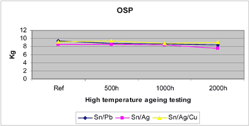


Figure 8:
Die shear results, NPO 1206 ceramic multilayer capacitor


Figure 9:
Die shear results, SOD 80 diode
The shear test of the wave soldered SMD components did not give usefull test results since the variation indicated that other parameters that the solder joint (mounting glue) influenced the strength. A following microscopy survey revealed that the variation was caused by the production process, where different amounts of glue and solder obviously influenced the strength of the joint.
3.6 Combined reflow and wave soldering
60 test boards were reflow soldered on one side at Bang & Olufsen and the wave soldered at HYTEK. The following analyse was carried out at HYTEK.
All test boards have been subject to X-ray examination in order to check the integrity of the solder joints by examining the collected X-ray films at low magnification using stereo microscopy.
The lead free through hole mounted components showed stress lines at 100x thermal cycling. No stress lines were observed on the components mounted with lead containing solders. The lead containing solder joints showed stress lines at 500x thermal cycling.
Microscopy of the solder finishes of SMD components showed no tendency to stress lines at 1000x thermal cycling, independent from the type of solder.
The microscopy showed no visible difference whether the soldering was made on OSP or NiAu board surface finish.
The shear test gave a rather big spreading in data indicating that other parameters than the solder joint itself affected the results. A following microscopy of the broken solder joints confirmed that the amount of SMD adhesive and the adhesive strength together with a variation in the amount of solder from the wave soldering process could have affected the test. The major results of the C1206 and SOD80 SMD components mounted on board having NiAu and OSP finish is shown in the below figures:

Figure 10:
Shear test results of lead free joints

Figure 11:
Shear test results of lead containing joints
Hand soldering using lead-free solder wire requires a slightly different approach. A higher temperature of the soldering iron tip is required as well as a longer pre-heat (3-5 seconds) of the solder pad and component lead before applying the solder wire. Therefore lead free hand soldering requires much heat (pre-heat may be required) and full wetting of the plated-through-holes is problematic. A solder iron set-up suitable for lead free soldering is required compared to traditional tin-lead soldering.
3.8 Production case
This lead-free production case was initiated to investigate and compare on a well known product the reliability of lead-free solder joints vs. lead-containing joints for the three soldering methods: reflow soldering, wave soldering and hand soldering. The case should also verify whether or not immersion tin solder pad finish was a usable alternative to SnPb HASL, when changing to lead-free soldering processes.
The PCB selected for the production case was an existing Power Supply Unit produced by SIMRAD since 2000. The PCB was a multi layer (4 layers) FR4 with SMD and through-hole components on topside. The SMD components were reflow soldered and nearly all through-hole components were wave soldered. Only two leaded power transistors were finally hand-soldered. A total of 36 boards were manufactured divided in three batchs. Please consult Appendix 1 for more details about the case.
After manufacturing the product went through visual inspection, temperature cycling and shear force test. None of these tests indicated any SMD solder joint reliability difference between the 3 batches. Also with the hand soldered through-hole component joints no clear differences were found, although one of the lead-free joints had indication of crack formation after 500 temperature cycles. However, on the wave soldered joints small cracks were seen on the lead-free process, in the micro sectioning performed immediately after the wave soldering; although they did not cause any circuit failures even after 500 temperature cycles. The lead-free solder joints seem harder and more brittle than the lead-containing joints. This indicates that stress relieve clinching on the component leads might become necessary to minimize coefficient of expansion of the different materials.
To verify the strength of the SMD solder joints in each batch, and the effect of the temperature cycling a number of 1206 capacitors were shear force tested. The average results for each batch are shown in the below figure:

Figure 12:
Average shear force results for 1206 capacitors
Also for the objective Immersion Tin as HASL alternative, none of the 3 tests indicated that immersion tin could not be used as an alternative to HASL, both in lead-free and lead-containing applications. Compared with HASL solder pads the immersion tin solder pads showed equal solder ability - both in the lead-containing and in the lead-free soldering processes. The top fillets generally seemed to float out equally on the pad on all 3 batches. The only difference noticed was, that at some through-hole top side solder fillets, a clear border line was seen between the solder fillet and the solder pad. Since the tin surface of the pad is very thin and chemically applied, the border line must be a natural consequence and must be purely depended on the flux application and spreading at the PCB top side solder pads. It must however be stressed, that the PCBs with immersion tin surfaces were only 1 – 2 weeks old at the production time and the impact of a long-term storage was not investigated in this production case.