Survey on Lead Free Solder Systems
7 Appendix 1: Pb-free production case
Brian Sloth Bentzen – Simrad Støvring AS / SMT in FOCUS
Lars Ebdrup – Grundfos Electronics A/S
Poul Juul – Hytek
Maks Rasmussen - Hytek
August 2002
7.1 Introduction
As well known, we are moving towards a European ban on the metal, lead. A draft proposal in the Restrictions on the Use of Certain Hazardous Substances in Electrical and Electronic Equipment (RoHS) directive, associated with the European Waste from Electrical and Electronic Equipment directive (WEEE), bans lead from electronic products. The date for this ban is somewhat unclear but should be January 1st 2006 or 2007. However, the Japanese electronic industry is leading and forcing this process of removing lead from electronic products. Some of the major Japanese manufacturers already has lead-free soldered products in the stores. So, besides the driving force from a future ban on lead, it could very well end up as a competition and sales parameter.
The Danish project "Lead-free Soldering Materials" was initiated to investigate the process and environmental issues involved in changing to lead-free production of electronics. The project partners were Bang & Olufsen, Grundfos Electronics, Simrad Støvring, Hytek, Delta, DTC and Technoconsult.
The Pb-free production case described in this paper was a part of the Danish project.
7.2 Case objectives
This lead-free production case was initiated to investigate and compare the "lead-free" solder joint reliability against lead-containing joints for the three soldering methods: reflow soldering, wave soldering and hand soldering, on a well-known product.
The case should also verify whether or not immersion tin solder pad finish was a usable alternative to SnPb HASL, when changing to lead-free soldering processes.
7.3 Case set-up
The PCB selected for the production case was a well-known and reliable PSU unit produced since 2000. The PCB was a multi layer (4 layers) FR4 with SMD and through-hole components on topside. The SMD components were reflow soldered and nearly all through-hole components were wave soldered. Only two leaded power transistors were finally handsoldered. See Fig. 1.
None of the SMD or leaded components were qualified for the higher temperature lead-free soldering process or checked for lead on the component terminals.
Three batches of 12 PCBs were separately produced. Batch 1 (control batch): Pb-containing on HASL PCB, batch 2: Pb-containing on immersion tin PCBs and batch 3: "Pb-free" on immersion tin PCBs.
Batch 2 was included in the case set-up to ensure, that poor solderability due to the immersion tin coated solder pads were not mistaken to relate to the lead-free process.
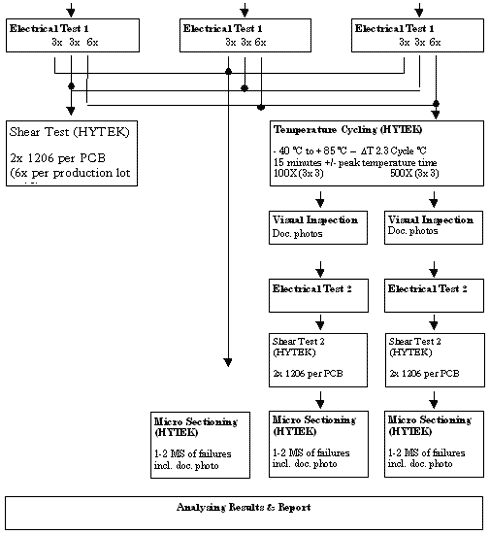
To verify the completed specimens against the case objectives, they were inspected visually, electrical tested, run through temperature cycling and shear force tested according to the schedule shown on the next page.
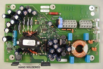
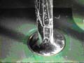
Fig. 1
PSU unit
7.4 Test schedule
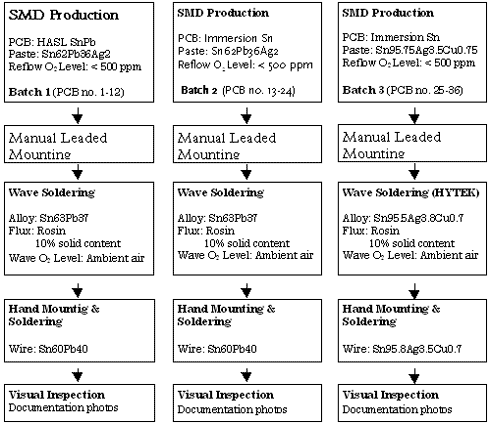
The screen printing of all 36 PCBs (18 panels) were performed on an off-line semi-automatic screen printer equipped with a manual vision system. A standard 150 m m (0.006") thick laser cut stainless steel stencil was used. All apertures were reduced by 20% in length and width.
7.6 SMD placement
All PCBs were processed on fully automated SMD placement equipment.
7.7 Reflow soldering
All 36 PCBs (18 panels) were reflow soldered in a medium size forced convection oven under nitrogen atmosphere. The rest oxygen level was < 500 ppm.
The two lead-containing product batches (1 and 2) were reflow soldered with the profile shown in Fig. 2 below. And the "lead-free" product batch (3) was reflow soldered using the profile pictured in Fig. 4.
The thermocouples were attached to 3 components on each PCB in the panel. See Fig. 3. The large coil L16 was the PCB’s cold spot which resulted in a fairly high peak D T. The solder paste alloy used was respectively Sn62Pb36Ag2 and Sn95.75Ag3.5Cu0.75.
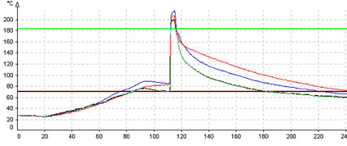
Fig. 2
Reflow profile for solder paste Sn62Pb36Ag2:
Preheat D T: ~ 2 – 3 ° C
Peak temperature: 208.8 – 234.8 ° C (D
T 26.0 ° C)
Time above melting point 179 ° C: 56.9 – 65 seconds
O2 < 500 PPM
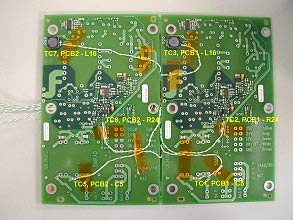
Fig. 3
PCB used in Reflow profiling
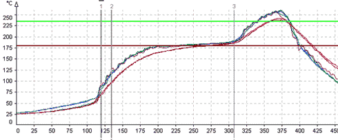
Fig. 4
Reflow profile for lead-free solder paste Sn95.75Ag3.5Cu0.75
Preheat D T: ~ 2 – 3 ° C
Time above melting point 217 ° C: 54.8 – 66.5 seconds
Peak temperature: 238.8 – 259.9 ° C (D
T 21.1 ° C)
Time above 235 ° C: 20.6 – 46.5 seconds
O2 < 500 PPM
7.8 Through-hole component mounting
All through-hole components were hand mounted by operator.
7.9 Wave soldering
In the lead-containing process, the flux was applied using a foam-fluxing unit. The wave-soldering machine, used in the lead-free soldering process, did not have a foam-fluxing system. The flux was therefor applied by dipping the populated PCB into a flux bath. The excess flux was removed with a paint roller. Earlier tests in the project indicated that synthetic and low solid content fluxes could not clean the solder lands etc. sufficient enough. So, an older 10% rosin flux was chosen for this production case. The solder alloy used was respectively Sn63Pb37 and Sn95.5Ag3.8Cu0.7.

Fig. 5
Wave soldering profile for Sn63Pb37 alloy
Solder pot temperature: ~ 250 ° C
Peak temperature: 204.8 – 215.6 ° C
Time above 183 ºC: 3.7 – 4.5 seconds
Conveyor angle: 7 º
Air environment
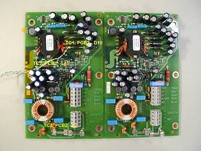
Fig. 6
PCB used in Wave profiling
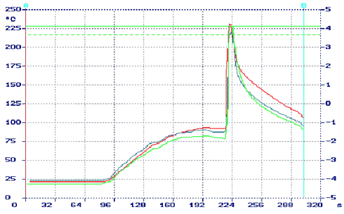
Fig. 7
Wave soldering profile for lead-free alloy Sn95.5Ag3.8Cu0.7
Solder pot temperature: ~ 270 ºC
Time above 217 ºC: 3.0 – 4.9 seconds
Peak temperature: 220 – 231 ºC
Conveyor angle: 6.5 º
Air environment
7.10 Hand soldering set-up
A standard thermostat controlled soldering iron, set to 400 ºC, was used to solder lead-containing solder wire. For the lead-free hand soldering a soldering iron with self-regulating soldering tip (400 ºC) was used. And the solder wire used was respectively Sn60Pb40 and Sn95.8Ag3.5Cu0.7.
7.11 Results and observations
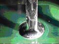
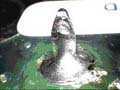
All PCBs were visually inspected after reflow soldering, wave soldering and hand soldering. There was a clear difference in the appearance of the solder joints. The joints soldered with the lead-free alloys were generally more dull and gray. But on this batch (3) there was also a huge difference found in the appearance, probably depending on the component terminal alloy or lead contamination (not verified). Compare photographs of Q13 and IC4 in Table 1.
Table 1
Visual comparison of SMD solder joints
|
Batch 1 |
Batch 2 |
Batch 3 |
PCB: HASL SnPb |
PCB: Immersion Sn |
PCB: Immersion Sn Paste: Sn95.75Ag3.5Cu0.75 |
|
C13, 1206 |
|
|
|
Q13, SOT 23 |
|
|
|
IC1 pin 1, Optocoupler |
|
|
|
IC4 pin1, SO8 |
|
|
|
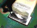
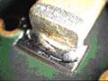
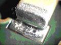
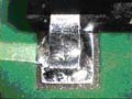
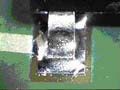
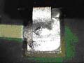
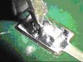
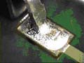
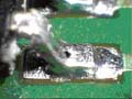
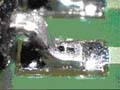
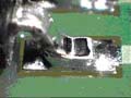
Table 2
Visual comparison of wave soldered through-hole solder joints
|
Batch 1 |
Batch 2 |
Batch 3 |
PCB: HASL SnPb |
PCB: Immersion Sn |
PCB: Immersion Sn |
|
|
|
|
|
R7 |
|
|
|

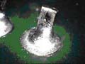
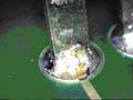
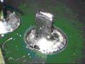
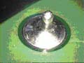
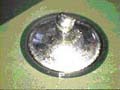
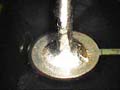
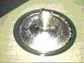
Table 3
Visual comparison of hand soldered through-hole solder joints
Batch 1 |
Batch 2 |
Batch 3 |
|
PCB: HASL SnPb Alloy: |
PCB: Immersion Sn |
PCB: Immersion Sn |
|
|
|
|
|
The 36 completed PCBs were electrical function tested. As seen below, two PCBs from the
"lead-free" batch 3, failed due to tombstoning and one missing component. These
PCBs were repaired and re-tested with positive results. 2x 9 PCBs were tested again
respectively after 100 and 500 temperature cycles with no additional failures detected.
Table 4
Result of electrical tests
Batch 1 |
Batch 2 |
Batch 3 |
|
PCB: HASL SnPb |
PCB: Immersion Sn |
PCB: Immersion Sn |
|
Electrical test 1 |
PCB failed = 0 |
PCB failed = 0 |
PCB failed = 2 (*) |
Electrical test 2 |
PCB failed = 0 |
PCB failed = 0 |
PCB failed = 0 |
Electrical test 2 |
PCB failed = 0 |
PCB failed = 0 |
PCB failed = 0 |
(*) PCB no. 27 failed due to R31 tombstoning. Repaired. Re-test was OK.
PCB no. 31 failed due to a missing component (D1). Repaired. Re-test was OK.
To test the solder joint reliability of the 3 batches, 2x 9 PCBs were exposed to a temperature cycle test; respectively 100x and 500x at 33 rH. See specification in Fig. 8. Earlier test performed, indicated a difference in joint reliability between lead-containing and "lead-free" joints after 500x temperature cycles. It was therefor decided not to continue the temperature cycling beyond 500 cycles.
Visual inspection of the 9 PCBs exposed to 100 temperature cycles initially showed no evidence of beginning joint degrading or cracking. However, even though the PCBs did not fail in the electrical function test after 500 temperature cycles, there was now clear evidence of crack formation on the wave soldered through-hole components. And the crack formations were seen on all 3 test batches. On the SMCs there were no indication of solder joint cracks whatsoever.
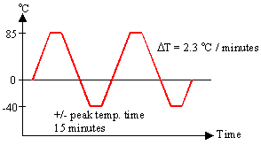
Fig. 8.
Temperature cycle profile
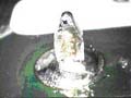
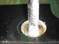
9x micro sectioning was done on 0805R (R21) and 1206C (C20), in the same cut; and 9x on a through- hole diode (D11). The micro sectioning revealed, that after 500 temperature cycles some SMD solder joints started to show some initial crack formations. See Fig. 9. These were seen randomly on the 3 batches. The micro sectioning also showed, as the visual inspections did, that all three batches had crack formations in the through-hole solder joints. It was also revealed, that minor cracks were already seen on batch 3 (lead-free process) at the D11 diode, immediately after wave soldering. See Fig. 10.
 |
 |
| Fig. 9. Crack in SMD joint - 500x temp. cycles immediately after wave soldering |
Fig. 10. Crack in "lead-free" through-hole joint |
To verify the strength of the SMD solder joints in each batch, and the effect of the
temperature cycling, 18 (totally 54) 1206 capacitors were shear force tested.
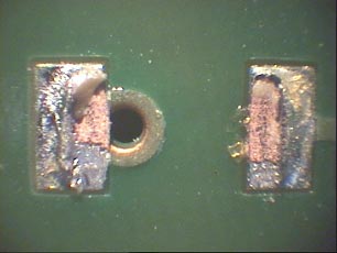
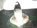
Fig.11
1206C solder joints after the shear force test
Fig. 11 shows the typical solder joint remains after the shear force test. It clearly indicates, that the separation is mainly seen between the com-ponent body and the terminal, although there also appear to be some separation between the solder fillet and the terminal.
The results of the tests are shown in the Fig. 12 diagrams. The 4th diagram shows the calculated average of each temperature cycling group of all 3 batches.
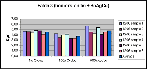
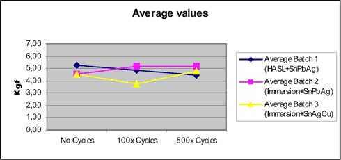
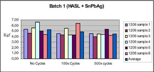
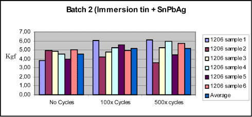
Fig. 12.
Shear force test results
As seen in the Fig. 12 diagrams, there was no clear evidence that one batch performed better or worse than the others. The deviation seen on the average calculation must be caused by the difference in the amount of solder alloy, the solder ability of the component terminals and test variations.
7.12 Conclusion
On the objective "Solder Joint Reliability", none of the 3 tests i.e. visual inspection, temperature cycling and shear force test indicated any SMD solder joint reliability difference between the 3 batches.
Also with the hand soldered through-hole component joints no clear differences were found, although one of the "lead-free" joints had indication of crack formation after 500 temperature cycles.
However, on the wave soldered joints small cracks were seen on batch 3 (lead-free process), in the micro sectioning performed immediately after the wave soldering; although they did not cause any circuit failures even after 500 temperature cycles. The lead-free solder joints seem harder and more brittle than the lead-containing joints. This indicates that stress relieve clinching on the component leads might become necessary to minimize coefficient of expansion of the different materials.
On the objective "Immersion Tin as HASL Alternative", none of the 3 tests i.e. visual inspection, temperature cycling and shear force test indicated that immersion tin could not be used as an alternative to HASL, both in lead-free and lead-containing applications.
Compared with HASL solder pads the immersion tin solder pads showed equal solder ability - both in the lead-containing and in the lead-free soldering processes. The top fillets generally seemed to float out equally on the pad on all 3 batches. The only difference noticed was, that at some through-hole top side solder fillets, a clear border line was seen between the solder fillet and the solder pad. Since the tin surface of the pad is very thin and chemically applied, the border line must be a natural consequence and must be purely depended on the flux application and spreading at the PCB top side solder pads.
It must however be stressed, that the PCBs with immersion tin surfaces were only 1 – 2 weeks old at the production time and the impact of a long-term storage was not investigated in this production case.
7.13 Hints
Screen printing of lead-free solder paste and SMD component placement on the lead-free deposits showed no complications whatsoever and no change in the processes were necessary.
For reflow soldering, a standard medium size forced convection oven was able to cope with the higher peak temperature, although it was necessary to reduce the soldering speed from 0.55 m/min to 0.45 m/min to reduce the peak D T. Depending on the mix of components on the PCBs, changing to lead-free soldering, longer and more powerful ovens may become necessary as might individual PCB profiling to minimize the peak D T due to the narrow peak temperature window. Vapor phase soldering could also be an option.
In the wave soldering process, individual temperature profiling will also become necessary. Selecting an appropriate flux showed to be the most important task. It seemed, that an older rosin flux gave a better result than a newer low solid content flux. However, wave soldering in a low oxygen (nitrogen) atmos-phere might help increase the process window and the usable flux selection.
Hand soldering using lead-free solder wire requires a slightly different approach. A higher temperature of the soldering iron tip is required as well as a longer pre-heat (3-5 seconds) of the solder pad and component lead before applying the solder wire.
The appearance of the "lead-free" solder joint might depend on the amount of lead contamination.
7.14 Contact information:
| Brian Sloth Bentzen
or Simrad Støvring AS Østre Allé 6 DK-9530 Støvring Phone: +45 99865152 E-mail: brian.bentzen@simrad.com Web-site: www.simrad.com |
Brian Sloth Bentzen SMT in FOCUS Birkagervænget 10, Godthåb DK-9230 Svenstrup Phone: +45 99865152 E-mail: brian.bentzen@smtinfocus.com Web-site: www.smtinfocus.com |
| Lars Ebdrup Grundfos Electronics A/S Birkevænget 2-10 DK-8850 Bjerringbro Phone: +45 87505513 E-mail: lebdrup@grundfos.com Web-site: www.grundfos.com |
Poul Juul Maks Rasmussen Hytek Dannebrogsgade 58 P.O. Box 519 DK-9100 Aalborg Phone: +45 98117003 E- mail: hytek@hytekaalborg.dk Web-site: www.hytekaalborg.dk |